Terafab Targets 1 Terawatt Annual Output in Aggressive 2028 Chip Production Plan
Musk claims equipment suppliers are accelerating deliveries for the Texas megaproject, aiming for high-volume manufacturing by late 2028.
By Kenji Hassan ·
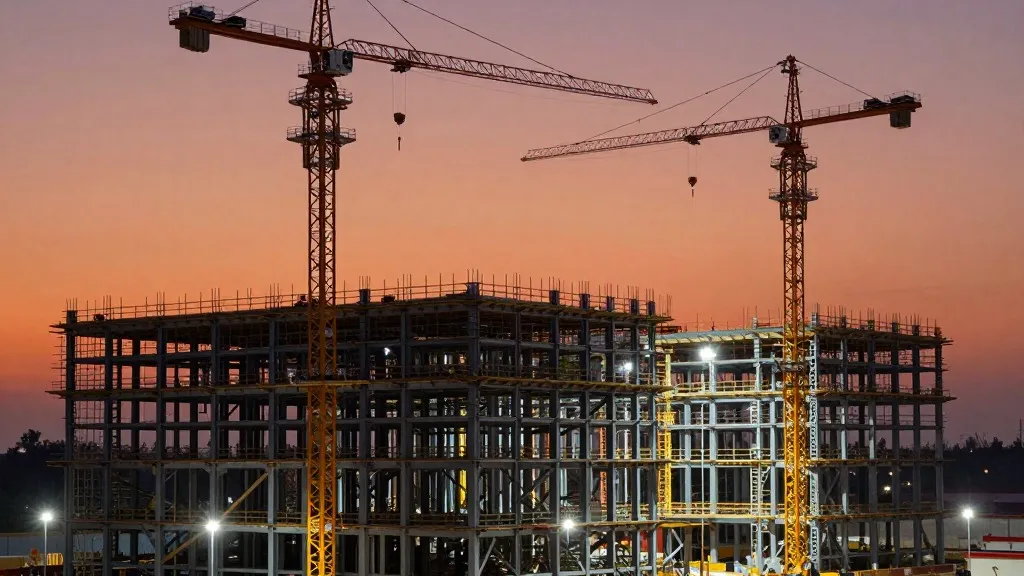
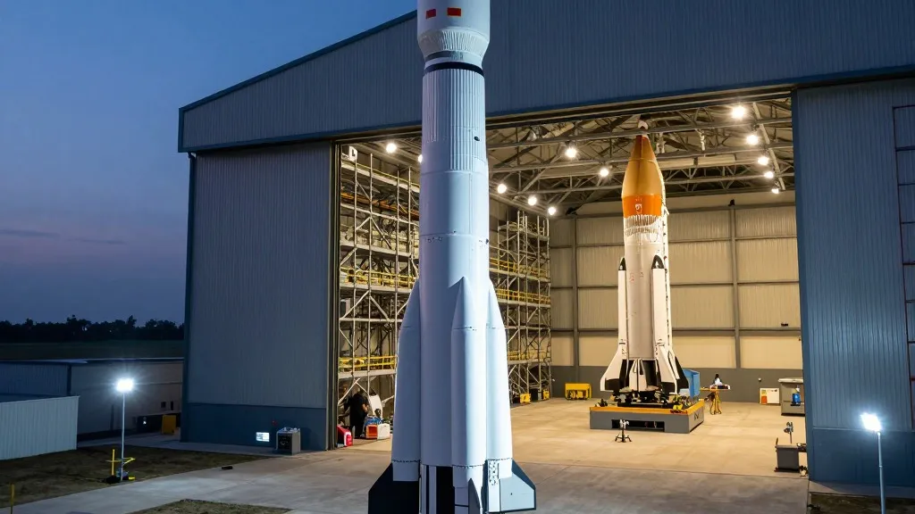
Elon Musk announced that critical semiconductor equipment suppliers, including ASML, are fast-tracking deliveries to support the rapid construction of Terafab. The facility, a joint venture between Tesla and SpaceX, is designed to manufacture advanced chips at a scale that Musk believes will rival the economic output of mid-sized nations. During a live broadcast of SpaceX's third-quarter 2026 earnings call on October 20, Musk outlined the ambitious timeline for the project, which is currently under construction in Gibbons Creek, Texas.
The primary goal of Terafab is to achieve volume chip production by the third or fourth quarter of 2028. Musk described this schedule as highly aspirational, noting that it carries significant uncertainty or large error bars. He expressed gratitude to suppliers for their willingness to accelerate equipment shipments to help meet these aggressive targets. The project represents a multi-billion dollar vertically integrated factory intended to produce logic, memory, and advanced packaging components under one roof.
The long-term vision for the facility involves generating one terawatt of AI computing power per year. If achieved, the commercial value of this output would place a single physical building within the top 20 global country GDPs. For perspective, Switzerland currently holds the 20th position with a GDP of approximately $1.14 trillion. This massive output is intended to supply Musk's xAI clusters, Tesla’s self-driving vehicles, Optimus robots, and SpaceX’s orbital data centers, while also addressing broader industry demand.
To reach these production levels, Terafab will utilize Intel’s 14A manufacturing node technology alongside traditional extreme ultraviolet lithography systems. Intel joined the venture in April 2026 to co-develop and refactor silicon fabrication processes. ASML, the exclusive commercial provider of the $400 million EUV machines required for leading-edge chips, is a central partner in this effort. Unofficial sources suggest the first EUV tool was originally slated for mid-2027 delivery, though it remains unclear if this aligns with the expedited timeline Musk referenced.
Beyond ASML, the project relies on a global supply chain that includes American firms Applied Materials, Lam Research, and KLA Corporation. Japanese manufacturer Tokyo Electron will also contribute front-end processing and metrology equipment. Additionally, Tesla and SpaceX are in negotiations with roughly ten South Korean equipment makers, including Hanmi Semiconductor and HPSP, for advanced packaging and specialized components. These collaborations are necessary to build the massive internal architecture of the factory.
Musk also provided updates on his AI computing ambitions during the same broadcast. He stated that his companies expect to have between 2.5 and 3 gigawatts of computing capacity active by the end of 2026. He expressed high confidence in adding an incremental 10 gigawatts in 2027, predicting a total of 13 gigawatts of AI compute by the end of that year. To achieve this, SpaceX and xAI are aggressively procuring next-generation Nvidia hardware, with plans to bring a 440,000-GPU Vera Rubin training cluster online by the second quarter of 2027.
The scale of Terafab raises questions about its feasibility in the current market. Research firm Gartner estimates that total global AI-optimized data center capacity is roughly 44 gigawatts as of late 2026. This figure represents only 4.4% of Terafab’s planned annual output. While global AI computing capacity has grown by roughly 3.3 to 3.4 times per year since 2022, experts remain skeptical of the one terawatt target. The project aims to mitigate future shortfalls from external foundries like TSMC, but the speed of construction is being scrutinized by industry analysts.
The next step for the project involves finalizing the supply agreements with the remaining South Korean partners and securing the earliest possible delivery windows for lithography equipment. The success of the 2028 timeline will depend heavily on whether suppliers can maintain their accelerated shipping schedules despite tight capacity across the semiconductor sector. If the initial experimental test chip, planned for the second quarter of 2027 at the Austin research facility, meets performance expectations, it will serve as a critical validation for the larger Gibbons Creek operations.
Source: Tom's Hardware · original report published